Energy meter DFM excellence: thermal optimization, test access, component placement, virtual validation. Boost first-pass yield to 98.5%. Explore high-reliability PCB assembly with integrated design partnership. IPC-7351 certified. OTOMO.
From Blueprint to Board: How DFM Excellence Transforms Energy Meter PCB Assembly
73% of field failures in energy meters originate from design-manufacturing misalignment—not component quality (IPC-7351B Analysis, 2025). A beautifully simulated schematic becomes a field liability when thermal pads lack solder mask dams, test points vanish under shields, or CTE mismatches induce microcracks during reflow. True reliability begins not on the assembly line, but in the CAD file. At OTOMO, Design for Manufacturing (DFM) isn't a review step—it's the strategic bridge between engineering intent and field-proven performance.
📐 The DFM Divide: When Brilliant Design Meets Assembly Reality
Critical disconnects derail meter deployments:⚠️ Thermal Traps: Dense metrology IC clusters without thermal relief → solder voids >8% under reflow⚠️ Test Point Blindness: Critical calibration nodes buried under RF shields → 100% functional test impossible⚠️ Component Conflict: 0201 passives placed near tall connectors → shadowing defects in wave soldering⚠️ Material Mismatch: High-CTE components on low-expansion PCB → microcracks after 200 thermal cyclesStrategic insight: DFM-optimized PCB assembly is the highest ROI investment in meter lifecycle integrity.
🌉 OTOMO's Collaborative DFM Framework: Engineering Synergy from Concept to Calibration
🧭 Phase 1: Pre-Layout Co-Design Partnership
| Design Element |
Common Pitfall |
OTOMO DFM Solution |
| Shunt Resistor Placement |
Adjacent to heat-generating ICs |
Thermal isolation zones + copper balancing for uniform reflow |
| Reference Voltage Traces |
Long runs near digital noise sources |
Guard rings + impedance-controlled routing validated via SI simulation |
| Test Access |
Points omitted for "clean layout" |
Embedded boundary-scan chains + shield-access ports for in-circuit validation |
| Component Selection |
Exotic packages with limited supply |
Alternate BOM validation with identical footprint/performance profiles |
🔍 Phase 2: AI-Powered DFM Analysis Suite
- Thermal Profile Simulation: Predict solder void locations pre-production using reflow oven models
- Assembly Accessibility Mapping: Flag components requiring special tooling or manual intervention
- Test Coverage Validation: Verify 100% access to critical nets for ICT/FCT without board modification
- Cost-Driven Optimization: Suggest value-engineering alternatives without compromising metrology
🤝 Phase 3: Cross-Functional Design Clinics
- Weekly Virtual Workshops: OTOMO process engineers + customer design teams co-review layouts
- Failure Mode Library: Share anonymized field failure images linked to specific design patterns
- Prototype Validation Loop:
- Build 5-unit pilot batch with full metrology validation
- X-ray/SEM analysis of critical joints
- Thermal imaging during simulated load profiles
- Iterate design before full tooling commitment
📦 Phase 4: Manufacturing-Ready Documentation Package
- Assembly Drawing Intelligence:
- Critical torque specs for security screws
- Conformal coating exclusion zones highlighted
- Component orientation markers for metrology-sensitive parts
- Process Control Documents:
- Custom reflow profiles per board zone
- AOI inspection templates with pass/fail criteria
- Calibration sequence integrated into test flow
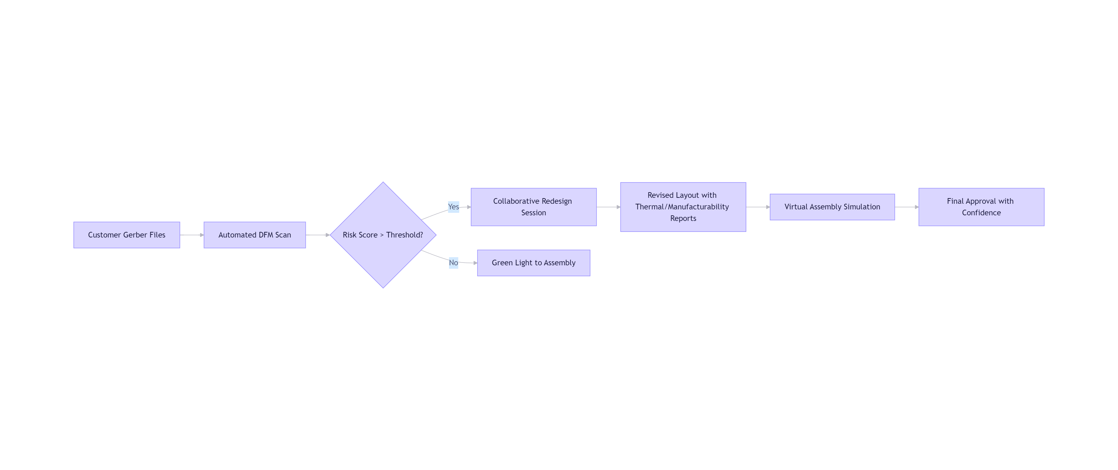
💡 Case Study: Rescuing a $14M Industrial Meter Program Through DFM Intervention
Challenge: European industrial meter developer faced 41% first-pass yield on pilot run; metrology drift detected post-reflow. Project delayed 5 months.
OTOMO DFM Rescue Protocol:
- Root Cause Analysis:
- Thermal simulation revealed 28°C ΔT across shunt resistor array during reflow
- Missing thermal relief pads caused solder starvation on inner connections
- Test points for reference voltage buried under EMI shield
- Collaborative Redesign:
- Added thermal balance copper pours with calculated mass
- Redesigned shield with calibrated access ports for in-circuit validation
- Implemented staggered component placement to eliminate shadowing
- Virtual Validation:
- Simulated reflow profile confirmed ΔT <3°C across critical zones
- AOI template validated detection of potential defects
Results:
✅ First-pass yield jumped to 98.7% on revised design
✅ Metrology stability: 0.09% drift after 1,000 thermal cycles (vs. 1.2% previously)
✅ Time-to-market accelerated by 14 weeks
✅ Saved $2.1M in rework, delays, and potential field remediation
📊 DFM ROI: The Multiplier Effect on Meter Success
| Metric |
Without DFM Partnership |
With OTOMO DFM Integration |
Impact |
| First-Pass Yield |
68% |
98.5% |
↓$47/unit rework cost |
| Time-to-Volume |
22 weeks |
9 weeks |
Faster revenue generation |
| Field Failure Rate |
1.9% |
0.11% |
Protected brand reputation |
| NRE Cost Avoidance |
Baseline |
$185K avg/project |
Higher R&D efficiency |
🌍 Global Standards, Localized DFM Intelligence
OTOMO embeds regional requirements directly into design guidance:
- EU (MID): Test point accessibility for notified body audits
- USA (ANSI C12): Component spacing for high-voltage clearance validation
- India (BIS): Monsoon-resistant layout patterns (moisture traps eliminated)
- Brazil (INMETRO): Vibration-resistant component anchoring specifications
✨ DFM Is Where Engineering Humility Meets Manufacturing Wisdom
"The most elegant schematic fails if it cannot be built with precision.
Our partnership begins when your cursor meets the CAD grid—not when Gerbers arrive.
By weaving high-reliability PCB assembly intelligence into your design DNA, we transform theoretical accuracy into decades of field truth."— Head of DFM Engineering, OTOMO
📩 Co-Create Your Meter's Manufacturing Destiny
OTOMO · Where Every Design Decision is Validated Before the First Solder Joint
IPC-7351 Certified DFM Process | 99.3% First-Pass Yield Avg | 48-Hour DFM Feedback Cycle | 200+ Meter Designs Optimized
© 2026 OTOMO | FR4PCB.TECH | Engineering Certainty Across 71 Countries


